Project Hub
/IoT & Connected Devices/Telemetry & Remote Logging/Kobee Studio – Modern PCB Graphics for KiCad
Advanced
AI / ML
Project Specific
Project Specific
Kobee Studio – Modern PCB Graphics for KiCad
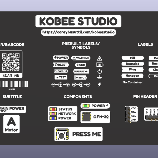
Kobee Studio is a feature-rich KiCad plugin for creating beautiful silkscreen graphics, labels, icons, connector overlays, QR codes, and PCB artwork directly inside the EDA tool.
We stock the boards, sensors and modules this project needs. A full parts list is coming soon — for now, browse our DIY Kits & components or search for AI / ML parts.
Kobee Studio operates as a specialized plugin integrated directly into the KiCad Electronic Design Automation (EDA) software suite. Instead of manually drawing complex vector graphics or struggling with external image conversion tools, users leverage the plugin to translate digital assets—such as custom logos, descriptive text labels, pinout diagrams, and machine-readable QR codes—into native KiCad graphical elements. When designing printed circuit boards (PCBs), visual data like silkscreen legends, component identifiers, and brand elements must be meticulously placed onto the board layers to ensure clear documentation and professional aesthetics. The plugin interfaces with KiCad's internal canvas and data structures, processing user-defined artwork and generating precise tracks, polygons, or silkscreen vectors that conform to the board's dimensional parameters. By handling the conversion process programmatically, the tool eliminates tedious manual layout tasks and maintains design file integrity, allowing hardware engineers and advanced makers to embed high-resolution graphics and schematics directly onto their physical hardware layers with exact placement and scaling.
Why Build This
Produce professional-grade, publication-ready PCBs featuring custom branding, clear connector overlays, and detailed pinout guides directly on the silkscreen layer.
Streamline hardware documentation and asset generation by embedding dynamic elements like QR codes and revision labels onto prototyping or production boards.
Enhance the aesthetic and functional layout of complex telemetry and IoT hardware projects for undergraduate engineering portfolios and commercial deployment.
Real-World Application
Streamlining PCB documentation, professional silkscreen labeling, branding, and asset generation for electronics manufacturing and hobbyist hardware projects.
Skills You'll Learn
PCB silkscreen optimization
EDA plugin workflow integration
advanced hardware documentation
visual asset layout
manufacturing layer preparation
Safety Precautions
No specific precautions noted for this build — always follow general electronics safety practices.
Technology Tags
KICAD
PCB DESIGN
PYTHON
SILKSCREEN
GRAPHICS EDITOR
OPEN-SOURCE
EDA
PLUGIN
Frequently Asked Questions
You need the KiCad EDA software installed along with the Kobee Studio plugin extension to access the design tools within your project environment.
Kobee Studio focuses on creating silkscreen graphics, labels, icons, connector overlays, and QR codes rather than functional electrical traces.
While accessible, it is targeted at undergraduate engineering levels and advanced users who are already comfortable with KiCad board layout and manufacturing layer concepts.
Gallery
This page is part of Kitkraft's Project Hub — a curated collection of electronics & robotics projects gathered from the maker community to help students and hobbyists discover and learn to build. Kitkraft does not claim authorship of the original project, and makes no representation as to the accuracy, completeness or safety of third-party source material. The summary and "How It Works" explanation above are AI-generated, rewritten with reference to the original tutorial — not a reproduction of it. Full credit and a direct link to the original source are provided above. If you're the original creator and have a concern about how your work is represented here, please contact us and we'll address it promptly.
Kitkraft Project Hub — curated from the maker community, credited at the source.