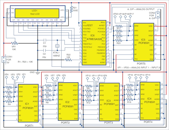
ATmega328 Analog I/O Port Expander Using I2C Bus
This project explains how to interface multiple PCF8591 ADC/DAC converters with an ATmega328 microcontroller using the I2C bus to expand the available analog inputs and outputs, displaying the results on an LCD screen.
Parts You'll Need
This project is sourced from another site, not written by us — this list is our best match of their components against what we stock, not a verified bill of materials. Always check the original blog (linked above) for the actual parts list before buying.
-
 10pcs - 220 ohm 1/4 W Resistor Set
Rs. 39.00
-
 Jumper Wire 10 Pin Male To Male 20cm
Rs. 45.00
-
 MB102 Adjustable Breadboard Power Supply Module (3.3V & 5V) for Arduino & Raspberry Pi
Rs. 139.00
-
 400 Points Mini Solderless Prototype PCB Breadboard High Quality
Rs. 89.00
-
 Jumper Wire 10 Pin Male To Female 20cm
Rs. 45.00


This list includes a generic resistor set as a placeholder — it is not matched to the exact value or part number this circuit needs. The correct one is specified on the original source page linked above; check it before buying.
We don't carry yet: LCD (generic / unspecified)
ATmega / AVR chip
ADC / DAC (ADS1115 / MCP3008 / MCP4725)
Custom PCB / PCB Fab
How It Works
Why Build This
Real-World Application
Skills You'll Learn
Safety Precautions
Technology Tags
Frequently Asked Questions
Gallery
This page is part of Kitkraft's Project Hub — a curated collection of electronics & robotics projects gathered from the maker community to help students and hobbyists discover and learn to build. Kitkraft does not claim authorship of the original project, and makes no representation as to the accuracy, completeness or safety of third-party source material. The summary and "How It Works" explanation above are AI-generated, rewritten with reference to the original tutorial — not a reproduction of it. Full credit and a direct link to the original source are provided above. If you're the original creator and have a concern about how your work is represented here, please contact us and we'll address it promptly.